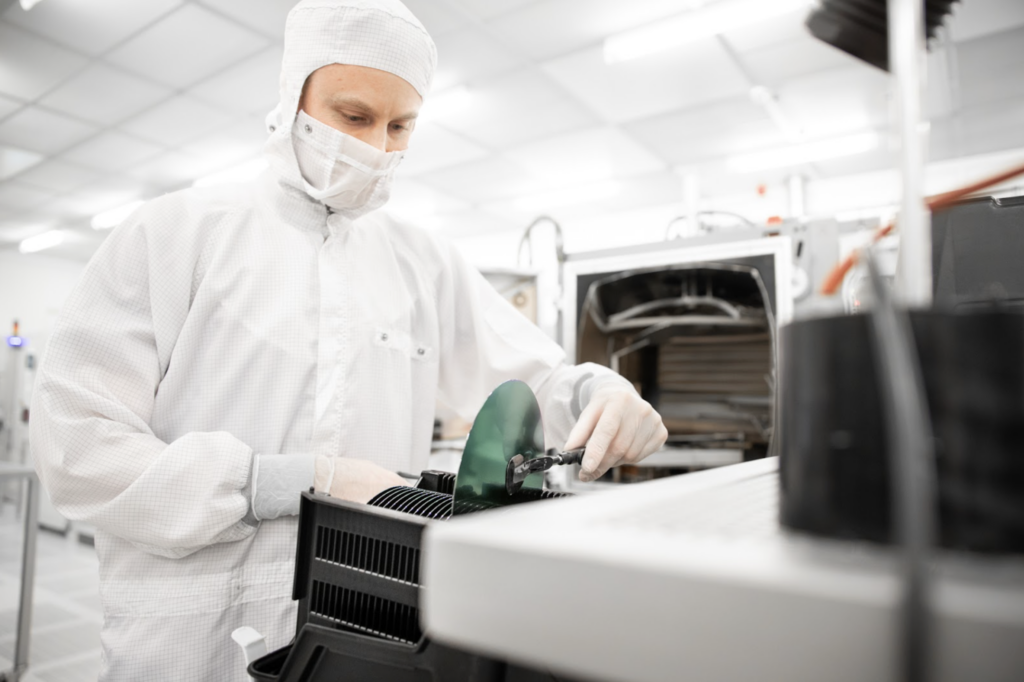
Frotech SASU develops equipment, materials and technologies for the production of power electronics on silicon carbide and advanced semiconductor materials, including modern technologies for cutting semiconductor ingots and wafers, grinding and polishing, as well as epitaxy (including SiC-on-SiC).
We develop and offer advanced technologies for the production of power electronics on silicon carbide and advanced semiconductor materials, including gallium nitride. Breakthrough technologies for laser cutting of semiconductor ingots and wafers allow achieving high-quality results economically and at high speed.
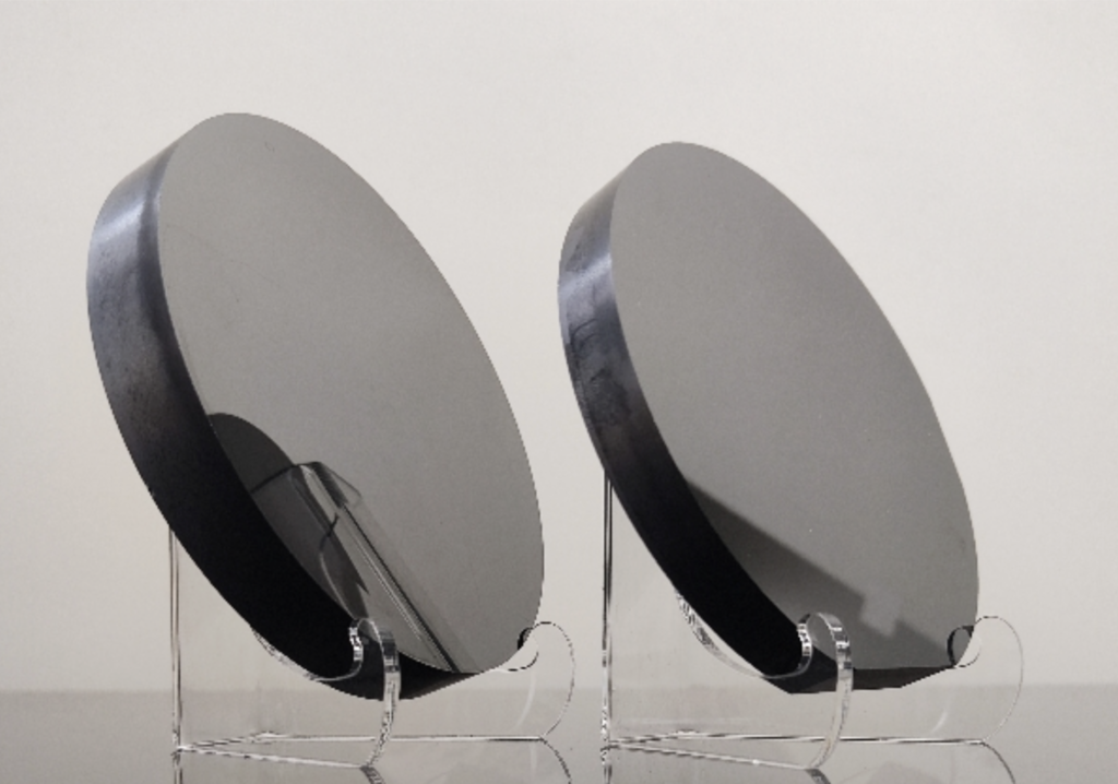
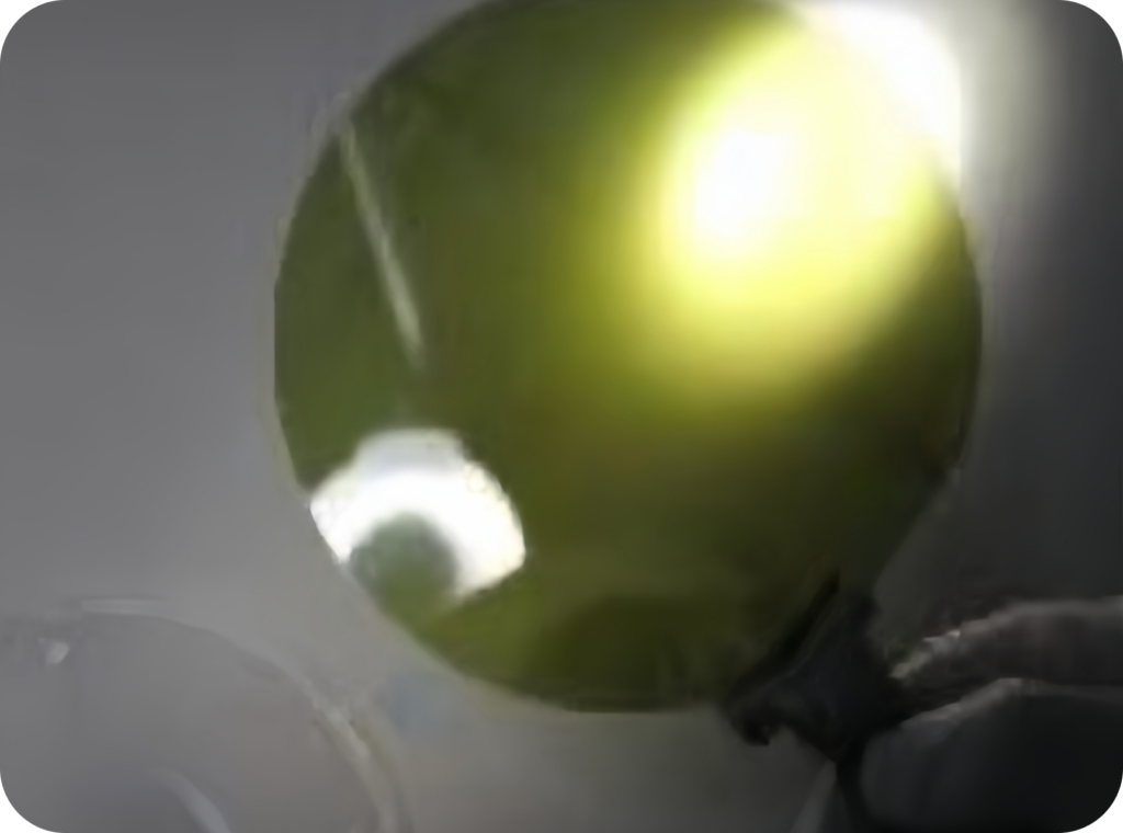
Epitaxy SiC-on-SiC
We are currently actively working on a number of innovative technologies in the field of micro- and nanoelectronics. In particular, we are focused on the development and improvement of equipment for processing semiconductor ingots and wafers of silicon carbide and other promising semiconductor materials, including laser separation and processing of wafers with a diamond tool.
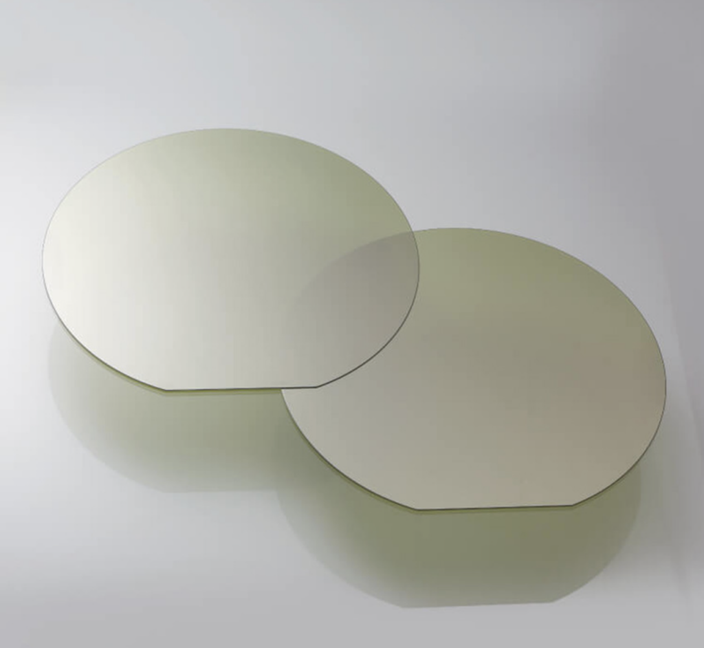
Epitaxy SiC-on-SiC
Services and maintenance
DEVELOPMENT AND MODERNIZATION
• Optimization of the design of serial models for individual customer tasks
• Modernization and retrofitting of customer equipment
• Conducting R&D on the development of vacuum equipment and key components of any complexity
TECHNOLOGICAL SUPPORT AND TECHNOLOGY TRANSFER
• Conducting test technological processes based on the Application Laboratory • Technological training and instruction of the customer's personnel • Development of new technological processes and their transfer to the customer as part of the equipment supply
TECHNOLOGICAL SUPPORT AND TECHNOLOGY TRANSFER
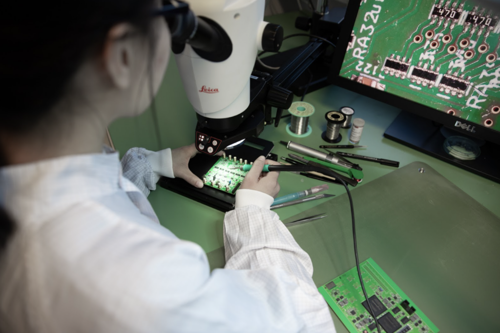
Application Lab
Application Lab was founded as Frotech division. It is equipped with all types of Frotech systems to carry out demonstration technological processes, as well as to confirm declared technical and technological characteristics of products. Experienced process engineers provide in-depth equipment testing and basic technological process development
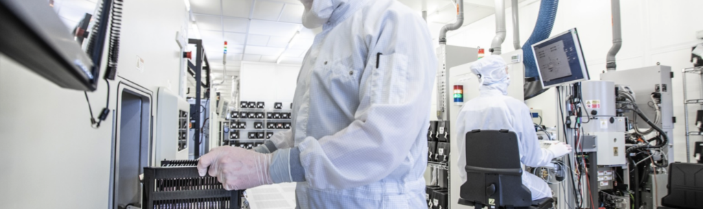
Equipment commissioning at the customer’s site includes end user training and setting up basic technological processes. It provides a quick start to production of heterostructures and semiconductor devices according to a given recipes.
Get in touch
Frotech SASU 2, Abel Antoune 33110 Le Bouscat Bordeaux France